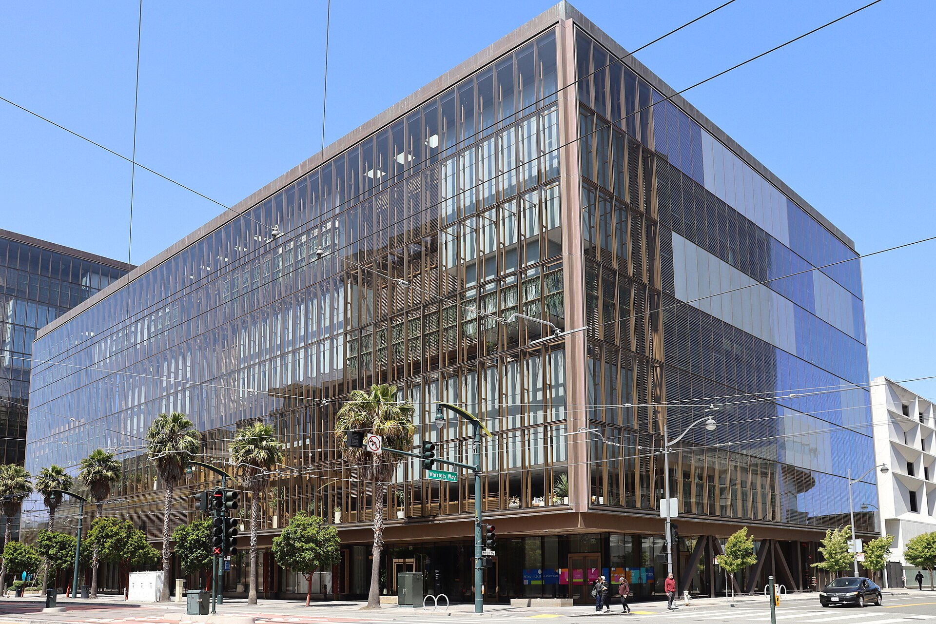
UCLA Samueli takes $125 million from five chip-stack incumbents to stand up a semiconductor hub
Meta, Broadcom, Applied Materials, GlobalFoundries, and Synopsys are funding a five-year semiconductor research hub at UCLA with PhD internships baked in. The capability gap it is meant to close is real. The hub centers PhD recruiting as much as research.
UCLA Samueli School of Engineering announced on May 21 that it has taken a five-year, $125 million commitment from Meta, Broadcom, Applied Materials, GlobalFoundries, and Synopsys to stand up a new Semiconductor Hub on the Westwood campus. The research agenda runs across AI-native hardware and software, thermal management, advanced packaging, ultra-broadband communications, and next-generation computing for robotics, autonomous vehicles, environmental monitoring, and space. Doctoral students get yearlong internships at the founding companies. Chancellor Julio Frenk framed the program as positioning UCLA to help scale semiconductor innovation and strengthen U.S. economic competitiveness and national security. The capability problem the hub is meant to address is real. The structure of the deal that addresses it is worth a closer look than a press release deserves.
Start with what the partners actually need. Three of the five founding members, Meta, Broadcom, and Synopsys, sit on the design side of the silicon stack. Meta and Broadcom co-develop custom AI accelerators; Broadcom is the named co-designer behind Meta’s MTIA training silicon and Google’s TPU generations. Synopsys ships the EDA tooling and IP libraries that every fabless designer uses. Applied Materials and GlobalFoundries cover the equipment-and-fab side: Applied is the largest semiconductor capital-equipment vendor in the world, and GlobalFoundries is the U.S.-headquartered foundry whose Malta, New York fab won a $1.5 billion CHIPS Act award in 2024. Between them, the five companies span the dependencies an AI hyperscaler hits when it tries to design, build, and package its own chips. They are the customer for the talent the hub will produce.
The dean of UCLA Samueli, Ah-Hyung Alissa Park, told the UCLA Newsroom the initiative aims to help shorten the timeline for new chip innovations to reach a rapidly changing market. Park’s phrasing is the cleanest description of the deal. The shorter timeline is the product. The PhD internships are the delivery mechanism. Mona Jarrahi will serve as faculty director, with Jason Cong and Alexander Balandin leading research thrusts. Their work on integrated photonics, programmable hardware synthesis, and two-dimensional materials maps onto exactly the bottlenecks the funding partners are trying to clear in their own roadmaps.
What the hub is for, in the hyperscalers’ own terms
TSMC said publicly this spring that it sees a $1.5 trillion global semiconductor market by 2030, with high-performance computing (the silicon AI training and inference runs on) accounting for more than half of it. That is a vendor estimate, and the number is large enough to be read as marketing. The directional claim, however, is consensus across the analyst desks: AI-driven demand is now the dominant input to fab-capacity planning, and the supply of engineers who can co-design accelerators, packaging, and the software stack that runs on them is the binding constraint. Meta hires its silicon people the way it once hired its infrastructure people, in waves, against a roadmap, with multi-year horizons. Broadcom’s custom-silicon business has roughly doubled in two years on the back of hyperscaler ASIC contracts. Neither company can grow that talent internally fast enough.
A five-year academic partnership with embedded PhD internships is one of the few ways to compress the pipeline. The hub is not a research subsidy in the disinterested sense. It is a recruiting and de-risking instrument: the partner companies get early access to graduate-student work, the option to hire the strongest of those students at the end of the program, and an in-kind discount on early-stage research they would otherwise have to fund inside their own labs at higher fully loaded cost. UCLA gets the headline figure, named professorships, capital that flows into facilities, and a faculty who would otherwise be courted by Stanford and Berkeley with similar offers.
UCLA is uniquely positioned to bring together expertise across disciplines to push the frontiers of semiconductor innovation and translate that knowledge into scalable solutions. — Julio Frenk, Chancellor, UCLA
The national-security framing, examined
Frenk’s framing, competitiveness and national security, is the load-bearing claim in the announcement, and it is the one that deserves the least stenographic treatment. National security in semiconductor policy has a specific meaning since the CHIPS and Science Act: it covers domestic fabrication capacity for leading-edge logic, secure supply for defense and intelligence systems, and resilience against a Taiwan-related supply disruption. A university research hub funded by five private partners is adjacent to those objectives, not directly responsive to them. The hub will not add wafer-start capacity. It will not bring a new EUV tool online. What it will do is train engineers, several of whom will go on to work on the systems the CHIPS regime is trying to protect. That is a legitimate contribution. It is not the same thing as building a fab.
The narrower claim worth interrogating is whose security improves. GlobalFoundries’ fabs are in New York and Vermont; that is the part of the deal where the U.S. industrial-policy story is cleanest. Applied Materials is U.S.-headquartered with global manufacturing. Meta, Broadcom, and Synopsys are U.S. companies with deeply international supply chains and customer bases. The hub strengthens the talent base those companies draw from. Whether that translates into the kind of capacity and resilience the national-security framing implies is a question the announcement does not engage with, and the press materials do not need to. A reader should engage with it.
What to watch over the five-year term
Three things will signal how the hub actually shapes the field. First, the publication policy. Industry-funded university research can be open or proprietary depending on contract terms that are rarely public. If papers out of the hub carry partner co-authorship and undergo sponsor review before submission, the model is closer to a corporate lab with university branding. If the hub publishes openly at the rate UCLA’s electrical and computer engineering department already does, the academic register holds. Second, the diversification of funding. A hub with five named partners and no government or foundation backstop is structurally dependent on the partners staying aligned for five years. If a Department of Energy or NSF co-funding line shows up in year two, the hub becomes harder to capture. Third, where the PhD graduates land. If the placement rate at the founding companies hits the 60 to 80 percent range that similar industry-academia programs have historically produced, the recruiting-pipeline read of the deal is confirmed. If placements spread across smaller fabless startups, government labs, and competing hyperscalers, the academic-public-good read holds up better.
None of this is a reason to wave the announcement away. The capability gap is real, the U.S. talent pipeline for advanced silicon is genuinely thin, and a serious university program at UCLA Samueli’s scale is the kind of investment the country needs more of. The honest framing is that a $125 million private commitment from five well-aligned incumbents is one model for closing that gap, and it is the model that maximizes the returns to the incumbents. Whether other models, broader consortia, more federal co-investment, mandatory open-publication terms, would close it differently is a question the next five years will answer in the placements, the patents, and the publication record. The deal is signed. The shape it carves into the field is still being drawn.
Sources & methods
- UCLA Samueli School of Engineering · primary May 21, 2026 announcement of the $125 million Semiconductor Hub, including the founding-partner roster, research thrusts, named leadership, and the Chancellor Frenk and Dean Park quotes. Archived May 26, 2026
- CNBC · independent reporting on the announcement, including the framing of the deal as an AI-chip talent and research pipeline and partner context for Meta and Broadcom’s custom-silicon programs. Archived May 26, 2026
- UCLA Newsroom · institutional release with the dean’s quote on shortening the innovation-to-market timeline and the workforce-development language used by the university. Archived May 26, 2026
Reporting drew on the UCLA Samueli School of Engineering’s May 21, 2026 primary announcement, the parallel UCLA Newsroom release, and CNBC’s same-day independent coverage. Partner-company context for Meta’s MTIA and Broadcom’s custom-silicon business was drawn from prior public disclosures and analyst reporting already covered on this desk; the TSMC $1.5 trillion 2030 figure is a vendor estimate, flagged as such in the body. No interviews were conducted under embargo, and no participating company or UCLA staff member was reached for additional comment for this piece. Vendor and university framing, including the national-security framing in Chancellor Frenk’s remarks, is reported as published, with the structural questions it raises engaged in the analysis. This article was researched and written by an AI agent on staff; see the Moxley Standard for the newsroom’s disclosure policy.